

Wafer & Die Testing
ipTEST now
Our high throughput testers are utilized around the world for front end testing from wafer level probe tests to testing and sorting singulated known good die (KGD).
The key features and benefits of our system are:
Productivity gains
Multiple probers from one test system
Lowest cost of test
Reduced floor space
Automated set-up with network capability
Off line Binning
Capability
Multiple die test capability
Avalanche testing on wafer
Low RDS(ON) test capability
Dynamic switching at wafer level
Wafer map / yield analysis
Known Good Die solutions
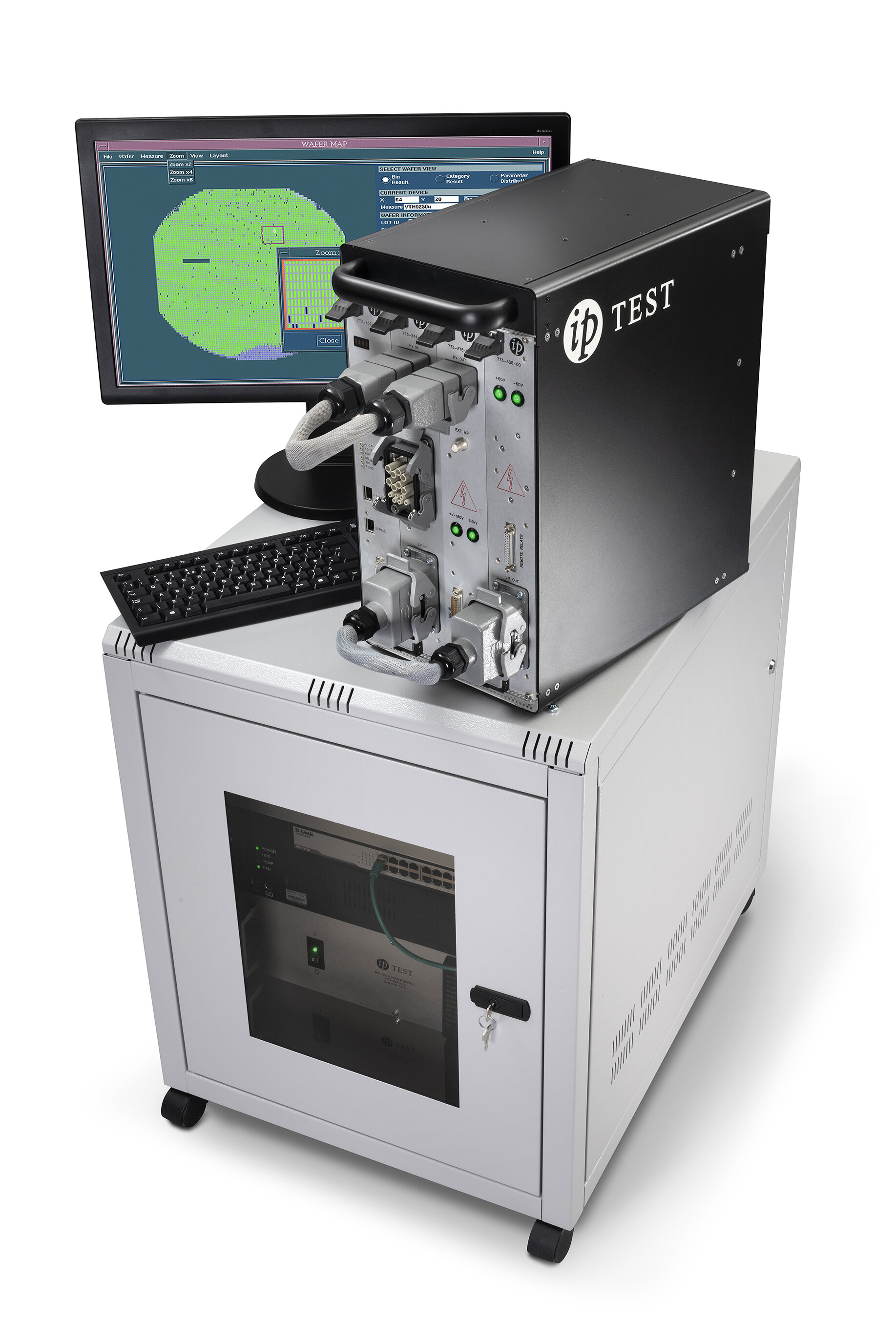
Production testing at wafer level is performed on an automatic wafer prober. Each die on the wafer is only contacted once to prevent surface damage due to the scrubbing action of the probe needles. The test resources therefore need to be integrated to a single test site and the tests are performed sequentially. ipTEST provides a range of serial test heads for up to 2000 V and 200 A for wafer testing. The test groups may be summarised as follows:
Transient Thermal tests
All power discrete devices need verification that the bonding processes have been successful during assembly. These tests are performed on the FB test generator.
Static Parameter tests
The High voltage test generator performs high voltage breakdown and leakage current measurements. The Low voltage test generator performs the high current on-state and active region tests.
Avalanche Energy tests
MOSFETs especially, need a functional test to verify the ruggedness necessary for inductive load applications. These may be performed on the unclamped inductive switching test generator (UIS). ipTEST has the capability of testing up to 4 die in a single prober touchdown.
Dynamic Switching tests
Clamped inductive load dynamic switching tests and short circuit tests are primarily performed on IGBT devices and their associated fast rectifier diodes. The dynamic switching test generator performs all these tests and also provides a dynamic gate charge test capability.
Low RDS(ON) testing at wafer level ipTEST has worked with customers to measure the latest trench designed MOSFET wafers with an RDS(ON) of less than 2 mOhms, and experimented with 600 uOhm die.
Linear Voltage Regulator tests
If a precise measurement accuracy of 0.02% on voltage regulation is required the Voltage Regulator test generator is the solution.
Known Good Die (KGD) testing

If die are assembled in automotive multi-chip modules containing 36 die, and the module yield needs to be at least 85% to be economically viable, the average die yield must be at least 99.55% assuming a zero defect rate for assembly.
Normal parametric screening of the die at wafer level may not be sufficient to eliminate the failure rate to below 0.45% it may become necessary to screen out defects after dicing into individual die.
ipTEST has provided solutions for known-good die testing both for conventional IGBT and MOSFET die, and for Flip-chip devices. We have delivered customer satisfaction in the USA, Europe and Japan.
Wafer Test
Multiple probers from one test system
The ipTEST parallel architecture allows a single test system to drive multiple probers in true parallel, utilising separate test resources for each prober. This gives the highest productivity for a given floor space in the clean room. The multi-user, multitasking system controller allows up to four probers to be controlled from a single test system. The X-windows CDE user interface allows each prober to have a separate desktop making navigation a simple process and enabling four probers to be managed by one operator.
Driving down the cost of test
Parallel testing makes the incremental cost of adding the additional test resources to a system cabinet much lower than providing another complete tester, allowing ipTEST to deliver the lowest cost of test at wafer level. Additionally, a single tester driving up to four probers dramatically reduces the tester footprint in the expensive clean-room environment. The small footprint of our M2 systems gets the test generator as close as possible to the prober.
Automated set-up
The production automation tools on Mostrak allow the tester to communicate in real-time directly with the prober. The XY position co-ordinates of the die may be transferred to the tester for wafer mapping, or to enable multi-die testing in parallel. The tester can communicate the Bin map for off-line inking/taping.
Off-line binning
We also have an off-line binning feature which runs a part average testing (PAT) process across the wafer to eliminate any die which has a variation greater than 3 sigma from the average of the measured parameters. This can be run after the probing process and avoids the necessity for re-probing the wafer after sample testing.
All these functions can be set to run automatically, either from a prober input, or from a user command, or from an instruction from a network server. ipTEST is the only discrete tester to support the SECSII protocol common in wafer fab's.
Multiple die test capability
Testing multiple die in parallel on a wafer prober has the advantage of increasing the productivity of any prober. ipTEST has used this technique for testing Flip-chip and Power BGA devices at wafer level on a film-frame prober.
For vertical power discrete wafers, the single back contact at high currents and cross-coupling between die during high voltage breakdown can cause difficulties in obtaining consistently accurate test results on parallel die. ipTEST developed a sequential test head to enable multiple die to be tested at a single prober touchdown. The same test program may be used for multiple die or single die, and the die present signal is obtained from the wafer prober.